Re: Cover Story: SilTerra surges ahead with silicon photonics | The Edge Markets
posted on
Jan 19, 2021 04:32PM


Wow !!! sometime I'm just amazed at how a poster react to another poster!
The intention from Oiposter was too highlight that another player in the field was making the headlines.
Those in the know, well those who been here for a long time or actually did some real DD were all aware that Silterra is part of the Poet Interposer platform ecosystem.
In fact, I do not care about your intention, bashing or pumping but I'm so happy that you pointed out that article despite you imminent lack of knowledge of Silterra direct relation to Poet.
I red the artcile and here is an abstract for all of us to "speculate" on that European tier 1 custormer.
Enjoy !
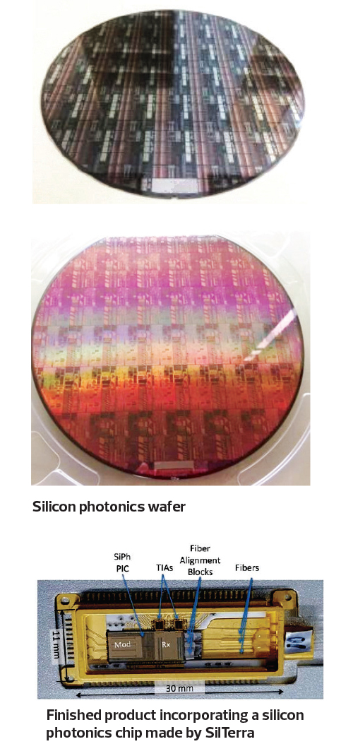
Silicon photonics chips are made of silicon but conduct photons instead of electrons, says Tan. “Their structures need to be adapted for guiding photons, also known as waveguides, very much like how a fibre-optic cable transmits light. Combining waveguides with semiconductors on the same wafer is the capability we have developed.”
As mentioned before, this is an incredibly difficult process and word got around that SilTerra was one of the few, if not the only one, that could do this. Lux Photonics Consortium programme director Dr Soo Choi Pheng says, “Silicon photonics uses light to move huge amounts of data at very high speeds, and SilTerra provides the right facility to support IC (integrated chip) product designers in realising their innovation to make this not only faster but also propagate to a wider range of applications.”
Then, customers started to come a-calling. “The killer app, as I said, is still data centres, but some are looking to use it for optical networking (a communications system that uses light signals instead of electronic ones to send information between two or more points),” says Tan.
Here is how it works. “The customer, such as Nokia, works with us to develop chips for its applications and we manufacture these for the company. We also partner with companies such as Packaging Technologies GmBH (PacTech), which has been appointed by these customers to package the chips into modules to sell to network companies such as Nokia, which, in turn, market them to data centre companies. Obviously, in the early stages of the market, only the biggest ones can afford them.”
Nokia’s chief technology officer for optical subsystems Michael Hochberg says working with SilTerra for the past several years has been a positive experience for the company. “We’ve been extremely impressed with their capabilities in terms of repeatability and process control, and their relentless focus on customer success. When we started working with them, we were a very young company and it was critical for us to focus on building up a process where we could build highly differentiated silicon photonic chips.
“Since then, we’ve built parts for both telecommunications and intra-data centre applications at speeds of 400G and beyond. I’ve developed processes in a number of fabs over the years and I’m consistently impressed by the SilTerra team’s responsiveness and eagerness to help.