Copper Wires Have Already Failed Clustered AI Systems
posted on
Sep 13, 2024 01:36PM


https://www.nextplatform.com/2024/09/13/copper-wires-have-already-failed-clustered-ai-systems/
It has become a well known fact these days that the switches that are used to interconnect distributed systems are not the most expensive part of that network, but rather it is the optical transceivers and fiber optic cables that comprise the bulk of the cost. Because of this, and the fact that optical components run hot and fail often, people have shied away from using optics except where necessary.
And so we have copper cables, increasingly driven directly off switch ASICs and the devices they connect, for the short haul and optic cables for the long haul that is necessary to provide the 1,000 or 10,000 or 100,000 devices required for AI and HPC systems. To which we quipped back in May when Broadcom launched its “Thor 2” network interface card chips and in the wake of Nvidia’s launch of the GB200 NVL72 rackscale system in March, use copper cabling when you can and use optical cabling when you must. The economics and reliability of the machines depend on this approach, both Broadcom and Nvidia will tell you.
The GB200 NVL72 system illustrates this principle taken to the most extreme. This system lashes together those 72 “Blackwell” GPUs in an all-to-all shared memory configuration with 5,184 massive copper cables, and the 200 Gb/sec SerDes in the nine NVLink Switch 4 switches at the heart of the NVL72 system can drive the 1.8 TB/sec NVLink 5 ports on each Blackwell GPU directly, over copper wires, without the need for retimers and certainly without the need for the optical transceivers used in long-haul datacenter networks. It is impressive, and saves somewhere on the order of 20 kilowatts of power compared to using optical transceivers and retimers, according to Nvidia co-founder and chief executive officer Jensen Huang, which drops the rack down to 100 kilowatts compared to the 120 kilowatts it would have been. (The original specs from Huang said the NVL72 weighed in at 120 kilowatts, but the spec sheets now say it is 100 kilowatts using all-copper interconnects for the rackscale node. We think added in the 20 kilowatts he saved by not using optics when he spoke.)
Anyway, this picture of the NVL72 node is enough to make you want to buy copper on the commodities market:
Mark Wade, co-founder and chief executive officer at Ayar Labs, which has created an optical I/O chip called TeraPHY and an external laser light source to drive it called SuperNova, is having none of this.
“I am making the argument that copper is already not working,” Wade explained to The Next Platform ahead of his keynote address at the AI Hardware Summit this week. “There is no company at the application level right now that is actually achieving significant economic output. It is not a question of when does copper fail and when does optics have cost parity and become reliable. Copper has already failed to support the AI workload in an economical manner. Yes, there has been two years of an investor-funded gold rush that that really fueled all of the all the profits coming into the hardware of players. But copper has already failed in supporting efficient, cost effective, performant systems for the AI workload. The industry is actually trying to dig itself out of a situation to where the technology has already failed, and hardware builders need to dramatically increase the cost-effective throughput of these systems. Otherwise, we’re all heading towards a Dot-Com style crunch.”
Those are pretty strong words, obviously, especially considering the size and strength of the order book at Nvidia, AMD, Taiwan Semiconductor Manufacturing Co, SK Hynix, Samsung, Micron Technology for their parts of the GPU accelerator supply chain. But hear Wade out, because he will make an interesting case.
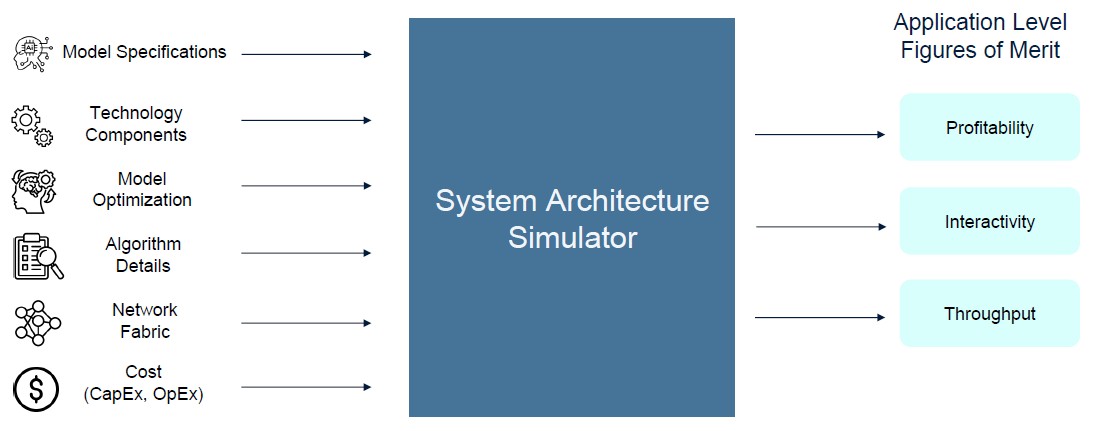
Ayar Labs obviously has a vested interest in compelling companies to move to optical I/O packaged onto GPUs and the switches that interconnect them, and to prove its point, the company has built a system architecture simulator that looks not just at feeds and speeds for various technologies, but their profitability when it comes to chewing on and generating tokens.
Now, Wade admits that this simulator, which is written in Python and which has not been given a name, is not a “cycle accurate RTL simulator,” but says that it is designed to bring together the specs for a whole bunch of key components – GPU speeds and feeds, HBM memory and capacity, off-package I/O, networking, CPU hosts, DRAM extended memory for GPUs, and so forth – and projects how various AI foundation models will perform and what their relative cost per token processed will be.
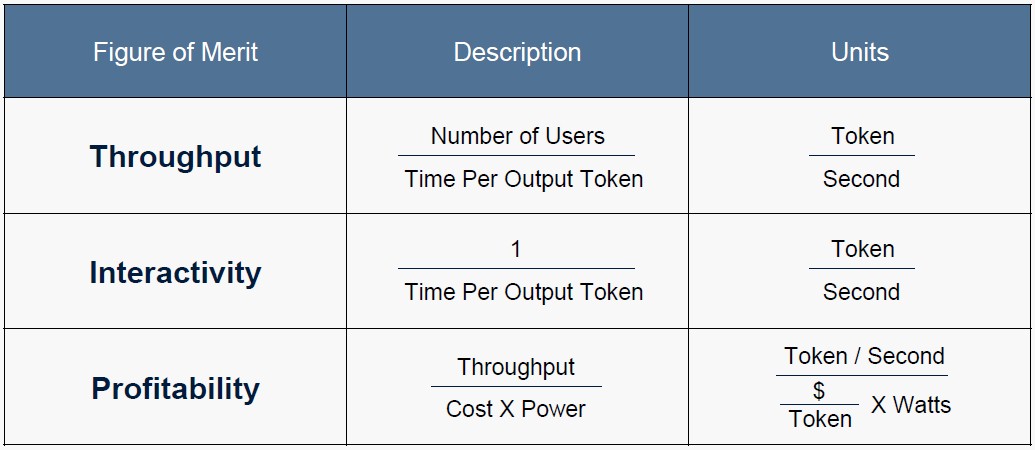
The AI system architecture simulator focuses on three figures of merit, not just the two that most people talk about. They are throughput and interactivity, which everyone is obsessed by, but also brings the profitability of the processing into the equation. Just as a reminder:
Obviously, Ayar Labs believes that all of the key elements of the AI cluster node – CPUs, GPUs, extended DRAM memory, and the scale-up switching within a node to link the GPUs – should use optical rather than electrical interconnects, and specifically AI servers should use its TeraPHY device pumped by its SuperNova laser.
But before we got into the system architecture comparisons, Wade added another layer to his argument, differentiating between three different styles of AI application domains. The first is batch processing, where groups of queries are tied up together and processed together like mainframe transaction updates from five decades ago. (Well, like mainframes do a lot during the nightshift even today.) The batch level of processing needs an interactivity level of 25 tokens per second or less. Human-machine interactions – the kind that we are used to with applications exposed as APIs that generate text or images – need to operate at 25 to 50 tokens per second. And the holy grail of machine-to-machine agentic applications, where various AIs talk to each other at high speed to solve a particular problem – require interactivity rates above 50 tokens per second.
This latter type of application is very difficult to attain on an affordable system that uses electrical interconnects, as the Ayar Labs simulator will show. And to be absolutely fair, companies like Nvidia are using electrical interconnects and copper wires in such a heavy handed way because there are still reliability and cost issues with individual optical components that need to be solved. But Wade says these are being solved and that its TeraPHY and SuperNova combo can intersect the generation of GPUs that will come out in 2026 and beyond.
With that said, let’s take a look at the feeds and speeds of the Blackwell GPU and how the future “Rubin” GPU on the Nvidia roadmap for 2026 and with a memory upgrade in 2027, might be architected the current electrical/copper way and a hypothetical optical/fiber way. Take a gander at this:
The Nvidia GB200 node has one “Grace” CG100 Arm CPU and a pair of Blackwell GB100 GOU accelerators, and so the compute capacity shown is half of what is on a spec sheet. It looks like the GB200 will be getting 192 GB of HBM capacity with the full 8 TB/sec of bandwidth, and the HGX B100 and HGX B200 cards will be getting Blackwells with only 180 GB of capacity. At least for now. The scale-up electrical I/O is from the NVLink 5 controller on each Blackwell chip, which has 18 ports that run at 224 Gb/sec and that provide 900 GB/sec of aggregate bandwidth both transmitting and receiving (so 1.8 TB/sec in total) for the Blackwell GPU.
Wade made some assumptions about what the Rubin GPU might look like, and we think there is a high probability that it will be comprised of four reticle-limited GPU chiplets interconnected by NVLink 6-C2C SerDes, much as Blackwell is two reticle-limited GPUs interconnected by NVLink 5-C2C SerDes. We know the Rubin HBM memory will be boosted to 288 GB and we and Wade both expect for the bandwidth to be boosted to around 10 TB/sec per device in the Rubin device. (It could boost further to 12 TB/sec in the Rubin Ultra kicker in 2027.) It is fair to assume that NVLink 6 ports will double the performance of the electrical interconnects once again to 1.8 TB/sec each way, and that could be by doubling up signaling per port.
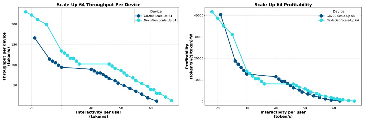
The Ayar Labs simulator swaps out the NVLink 6-C2C for its TeraPHY optical link, and by doing so, the bandwidth per direction goes up by a factor of 5.7X to 5 TB/sec. The simulator also assumes that NVSwitch 5 chips will double up their performance for the Rubin generation compared with the NVSwitch 4 ASICs used in the rackscale Blackwell systems and Nvidia will drive the electrical signals directly off the NVSwitch 5 chip again. And if you run these two hypothetical Nvidia scenarios through the Ayar Labs AI system architecture simulator and measure throughput and profitability – what we used to call dollars per SWaP back in the Dot-Com days, with SWaP being short for Space, Watts, and Power – across a range of interactivity, you get this pretty chart:
As you can see, moving from Blackwell to Rubin in 64 GPU systems with electrical signaling does not really move the needle all that much in terms of throughput at a certain level of interactivity, and the cost per unit of work per watt is not going to change all that much. It looks like Rubin will cost as much as Blackwell for a given unit of work, at least for the assumptions that Wade is making. (And this strikes us as reasonable, given that time is money right now in the upper echelons of the AI space.)
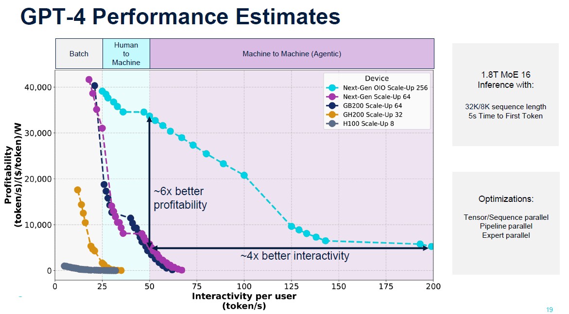
Now things are going to get interesting. Let’s look at how the GPT-4 large language model from OpenAI stacks up running inference in terms of profitability versus interactivity for different Nvidia GPUs at different scales in the Ayar Labs simulator:
This chart is fascinating.
First, it shows that an eight-way Hopper H100 node is acceptable for batch GenAI and barely able to do human-to-machine chatter. With a cluster of 32 GH200 superchips, which sport 141 GB of HBM3E memory, batch GenAI gets a lot less costly and the performance improves quite a bit relative to the smaller H100 node. The GB200 nodes with 64 GPUs start really bending the curves, but the difference between the GB200 and the future GR200 is not particularly discernable at 64 GPUs.
But look at what happens when Rubin comes out with optical I/O instead of electrical NVLink ports and electrical NVSwitch ports and the machine scales up to 256 coherent GPUs, which is not possible with copper cables because you can’t get that many GPUs close enough to each other to interconnect them. Machine to machine multi-model processing becomes not only possible. (Once again, we will point out: Don’t network the machines. . . . TeraPHY indeed.) The curve for the interplay of profitability and throughput for the hypothetical Rubin GPUs is incredibly better with optical I/O.
This chart suggests a few things: Ayar Labs is trying to get Nvidia to acquire it, or is trying to get Nvidia to uses its OIO chips, or tried and failed and is using this story to try to get AMD to buy it. Intel can’t buy a cup of coffee right now.
Now, let’s step up to the state of the art GPT model from OpenAI in 2026 or so, which we presume will be called GPT-6 but which Wade calls GPT-X just to be safe.
With GPT-X in 2026, the model will double up to 32 different models in is complex (called a model of experts), and Wade expects the number of layers in the model will increase to 128 from 120 with GPT-4. (We think the layers could be higher than this, perhaps as high as 192 layers; we shall see). The token sequence lengths will hold steady at 32k in and 8K out, and the model dimensionality for text embeddings will double to 20,480.
As you can see below, with the existing Hopper and Blackwell configurations scaling from 8 to 64 GPUs, all of the machines are shoved down into the batch performance realm, and only the Rubin rackscale machine with copper NVLink interconnects can even get into the human-to-machine realm. But with optical I/O in the node and across the nodes and with scaling up to 256 Rubin GPUs, Nvidia could build an inference machine that can scale human-to-machine and machine-to-machine realms while offering acceptable improvements in interactivity and cost.
That chart is an advertisement for Ayar Labs, Eliyan, Avicena, Lightmatter, and Celestial AI – among others. We strongly suspect that Rubin will move NVLink to optical interconnects, and frankly, we expected such a machine already given the prototyping Nvidia has done years ago and the work Nvidia has already done with Ayar Labs and quite possibly with some of the others mentioned above.
NVLink is just a protocol, and it is time perhaps to move it to optical transports. We can’t wait to see what Nvidia will do here. Cramming more GPUs in a rack and pushing the power density up to 200 kilowatts or the crazy 500 kilowatts people are talking about might not be the answer. Optical interconnects would space this iron out a bit, and perhaps enough to keep the optics from behaving badly.