Re: FD-SOI
in response to
by
posted on
Jul 20, 2015 05:21PM


Full article recomended:
http://www.anandtech.com/show/8223/an-introduction-to-semiconductor-physics-technology-and-industry/5
...

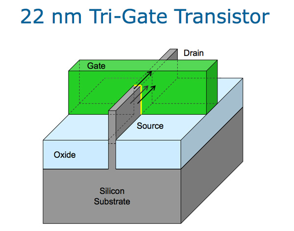
Unfortunately, once we get to 22 nanometers and below, short channel effects become even more significant. While we managed to decrease leakage and improve performance with HKMG, the gate still doesn’t have sufficient control over the channel because the gate keeps getting smaller relative to the substrate. The answer with the Tri-Gate transistor is to wrap the gate all around the channel that would form, dramatically reducing the amount of silicon far away from the gate. The resultant structure becomes like a fin, and due to the extremely thin channel the extent of the depletion region is determined by the physical structure rather than the applied bias to the terminals of the FET. This makes the transistor channel fully depleted as well, but this is merely an interesting side-effect, not a causative mechanism.
It's important to understand that this is why FinFET and FD-SOI are fully depleted technologies, but the key here is that the channel is now extremely thin so that the area far from the gate is eliminated. This means that the voltage and resultant capacitance of the gate should be able to overpower the effect of the drain's capacitance in all areas of the channel. The impact on performance is enormous.
As a result of this change, the off current is much lower than before as the effect of DIBL is reduced. This means that heavily doping the channel isn't necessary so variance in threshold voltages from one transistor to another is reduced. In addition, because of the larger inversion layer that can be generated and lower doping levels used in the channel, drive current is improved. This also means improved subthreshold swing can be achieved, so switching transistors on and off is even faster, which also improves performance. This is very much similar to the advantages that we see with FD-SOI, but it can be implemented on bulk silicon which reduces variable cost. FinFET and FD-SOI are just different ways of accomplishing the same goal, and share all the advantages of a thin channel.